SK hynix Launches Venture Capital Brand for AI Investments
Sep 18, 2026
Data Centers
SK hynix and Sandisk have unveiled the first standard specifications for High Bandwidth Flash, or HBF, announced in a press release. The announcement is tied to FMS 2026, held at the Santa Clara Convention Center from August 4 to 6.
HBF is a memory layer between HBM and SSDs. The specification covers capacities up to 512GB using 8 high and 16 high NAND die stacks, with bandwidth grades ranging from about 0.4 TB/s to 3.0 TB/s.
The standard uses the UCIe interface to connect HBF with processors, including GPUs and CPUs. It also covers connection interfaces, electrical characteristics, reliability, packaging guidance for die stacking, and software I/O guidance.
The specification was disclosed through the Open Compute Project Foundation. Google and Tenstorrent are participating in the HBF consortium.
SK hynix will also show its tenth generation V10 375 layer 4D NAND wafer and products at FMS 2026. The company says the NAND improves performance per watt by 2.5 times compared with the previous generation, and plans to begin mass production of high performance, high capacity eSSDs based on it early next year.
Consider subscribing to one of our newsletters like Silicon Brief or Daily AI Brief.
Also, consider following us on social media:
Weekly coverage of AI hardware developments including chips, GPUs, cloud platforms, and data center technology.

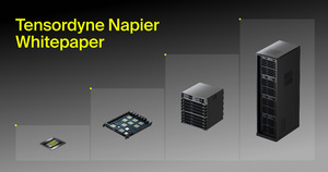
 Tensordyne
This Tensordyne whitepaper presents Napier, an inference-focused AI processor and rack-scale system based on the company’s TDN Math logarithmic number system. It examines infrastructure requirements for large mixture-of-experts and agentic models, compares major inference architecture approaches, and details the TDN AIP processor, TDN72 pod, TDN Link fabric, and Napier Ultra configuration. The paper reports simulation-based performance, cost, and accuracy-validation results, including Tensordyne’s projected comparison of one Napier rack with a nine-rack Nvidia Rubin plus Groq deployment; the chip is reported as taped out and in fabrication.
Read moreDaily AI Brief: the AI news that matters, in your inbox.